
From 800G backbone optical transceivers and 6G mmWave front-ends to automotive LiDAR and frontier quantum devices, InP is defining the boundaries of next-generation semiconductors.
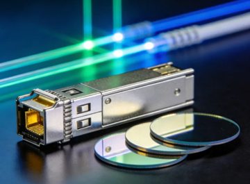
High-speed optical transceivers for AI data centers (800G/1.6T/CPO), long-haul fiber transmission, and 5G/6G optical fronthaul; used for DFB lasers, EML modulators, photodetectors, and photonic integrated circuits (PIC), compatible with the 1310/1550 nm fiber communication windows.
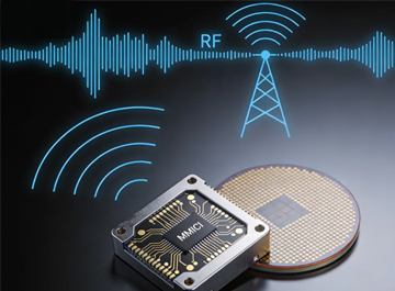
InP HEMT/HBT high-frequency transistors with low noise and high electron mobility; used in LEO satellite payloads, on-board RF amplifiers, mmWave communication, airborne phased-array radar, and electronic warfare, with strong radiation tolerance for space environments.
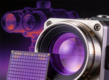
Focused on 1550 nm eye-safe automotive LiDAR, plus space laser communication, ranging, infrared detection, and single-photon detection; the mainstream substrate solution for high-end LiDAR light sources and receiver chips.
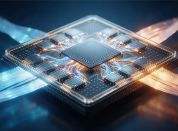
Space-grade high-efficiency multi-junction solar cells (space photovoltaics), plus quantum photonics (QKD, single-photon sources), terahertz imaging and inspection, and other frontier research and specialty equipment applications.
Filter InP substrates by size, doping, and resistivity, with real-time specifications and availability.
From cleanroom facilities and a specialized team to volume yield and quality systems, we deliver stable, reliable industrialization for InP substrate manufacturing.
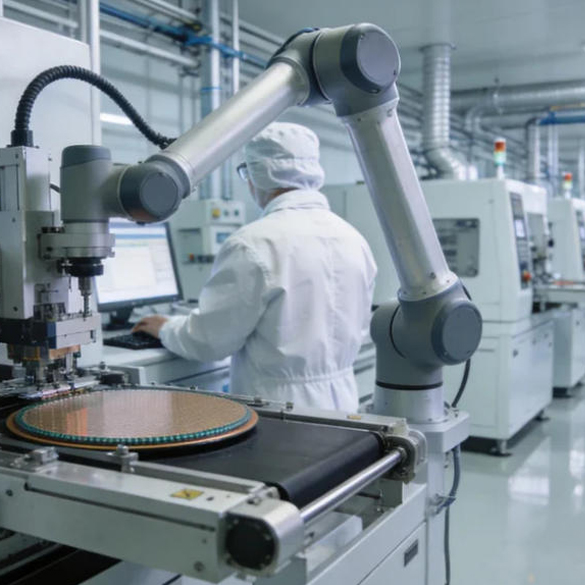
16,000 m² semiconductor cleanroom with ultrapure water treatment, meeting the stringent process environment requirements of compound semiconductor wafer manufacturing.
A senior team with deep experience in compound semiconductors and wafer equipment; R&D staff account for over 40%, with 20+ years of average industry experience.
Stable high-volume substrate production lines running at 300,000 wafers per year, with industry-leading batch consistency and yield.
ISO 9001 / ISO 14001, approved under customer qualified supplier systems, with full-process quality traceability.
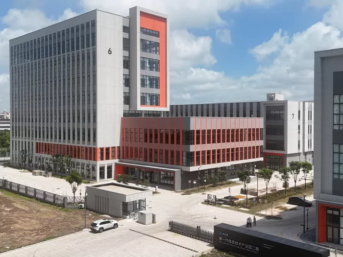
江苏芯光元晶体技术有限公司于2026年3月在江苏南通启东正式注册成立,专注于磷化铟衬底研发与制造。公司汇聚深耕化合物半导体、晶圆设备领域的资深技术团队,研发人员占比超40%。
企业拥有16000㎡ 现代化生产厂房,配套高等级半导体洁净生产车间,搭载专业超纯水处理系统,满足化合物半导体晶圆制造严苛工艺要求;现已建成规模化衬底量产产线,目前年产量可达30万片。
依托长三角成熟的半导体产业集群优势,企业聚焦光通信、射频半导体核心赛道,坚持自主技术突破,致力于打造国产化晶体材料与晶圆装备供应链,为国内半导体产业链提供高可靠国产配套方案,助力行业实现核心环节自主可控。
Company news, product launches, and industry insights, keeping you up to date on our latest InP developments.
The material of choice for high-speed optical communication, AI data center interconnects, and advanced sensing applications.
Tell us your requirements and our technical team will respond within one business day with samples and customized solutions.